

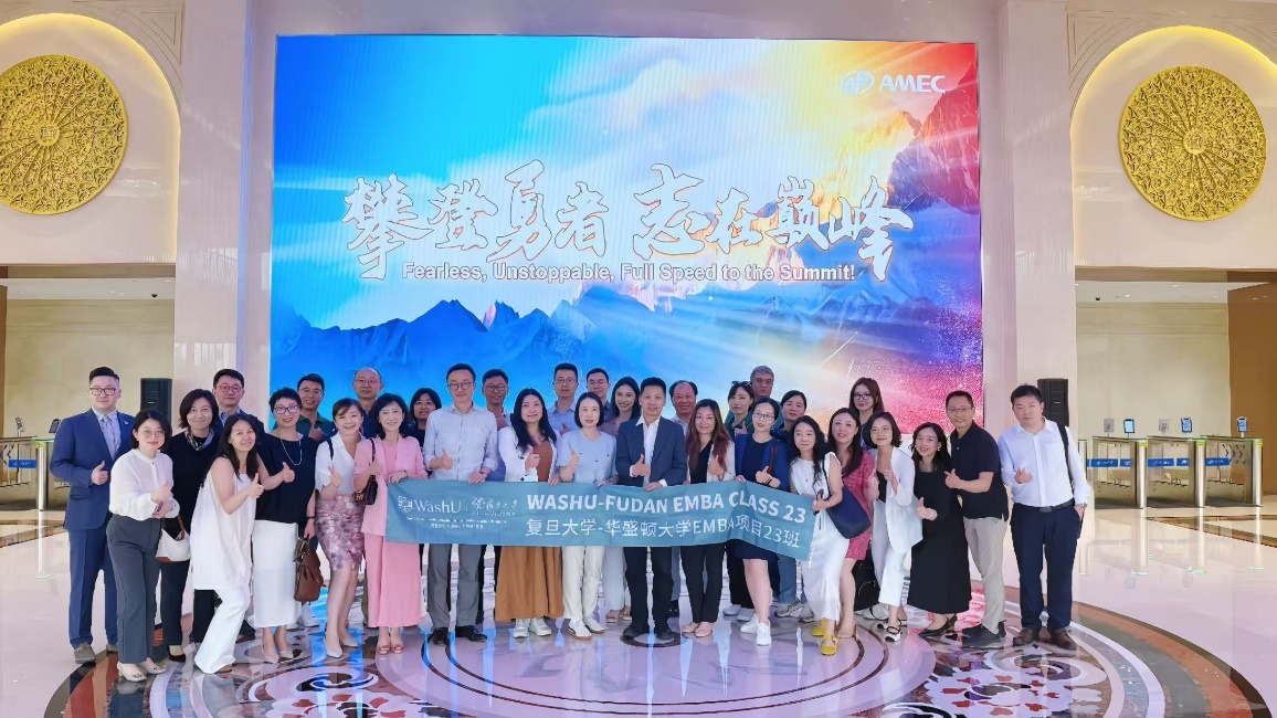
Recently, faculty and students of the Fudan-Washington University EMBA Program, led by Professor Feng Tianjun, Assistant Dean of Fudan School of Management and Professor in the Department of Management Science, conducted an in-depth visit to Advanced Micro-Fabrication Equipment (Shanghai) Co., Ltd., a STAR Market-listed enterprise. Mr. Liu Fang, Corporate Vice President and Secretary of the Board of AMEC, and Mr. Zhang Yu, Senior Investor Relations Manager, held in-depth exchanges with the faculty and students covering topics including AMEC’s technology roadmap and industry landscape.
At the corporate introduction session, Mr. Zhang Yu from AMEC walked the group through the company’s history and the R&D journey of its semiconductor equipment technologies. Founded in 2004, the company was successfully listed on the STAR Market in 2019. As a high-end micro-processing equipment enterprise rooted in China with a global vision, AMEC is committed to delivering leading processing equipment and process technology solutions for integrated circuit and LED chip manufacturers worldwide.
The digital industry built upon microfabrication features an inverted pyramid hourglass structure. The output value of the digital industry accounts for over 40% of the total output value of global enterprises. The manufacturing of semiconductor microdevices forms the foundation of the digital industry, and semiconductor micro-processing equipment serves as the cornerstone for producing all types of microdevices. The global semiconductor equipment market is valued at approximately USD 100–150 billion and has continued expanding in recent years. It represents the critical bottleneck of the entire digital sector, which truly validates the ancient maxim: *“A workman must first sharpen his tools if he is to do his work well.”
The downstream clients of semiconductor equipment include many of the world’s leading wafer fabs, with end applications spanning mobile phones, AI, autonomous driving and other sectors. The semiconductor industry now faces multiple favorable growth drivers; the global semiconductor market is expected to exceed one trillion US dollars within the year. Demand for memory and logic chips is currently on an upward trajectory. Mainland China hosts the world’s largest market for front-end integrated circuit equipment, accounting for 38% of global demand in 2025. Achieving self-reliance and controllability within the semiconductor equipment industry has become essential to safeguarding industrial development and consolidating the foundation of science and technology.
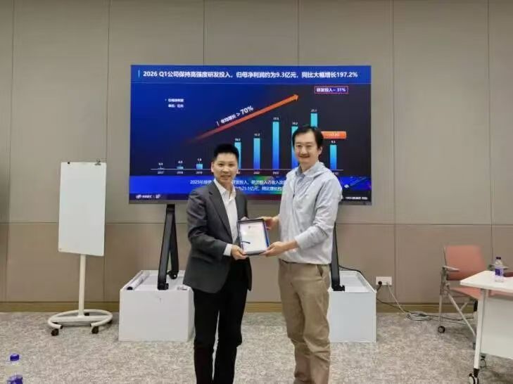
Mr. Liu Fang, Secretary of the Board and Corporate Vice President of AMEC, delivered an in-depth presentation covering AMEC’s technology roadmap and development strategy. Drawing on industry data and cutting-edge technologies, he comprehensively analyzed the current state of the sector and the company’s growth journey, allowing faculty and students to gain first-hand insight into the core competitiveness and growth potential of domestic high-end semiconductor equipment enterprises.
AMEC’s etch equipment has been widely adopted by leading domestic and international clients, supporting a broad range of etching applications from 65nm down to 3nm and more advanced processes. The company’s thin-film equipment sales saw explosive growth in 2025, emerging as a major new engine driving its performance expansion. At present, notable progress has been made in the localization of storage equipment for 3D NAND, while substantial breakthrough potential remains for mainstream DRAM and advanced logic chips. Going forward, through organic growth and external expansion, AMEC aims to cover over 60% of high-end critical integrated circuit equipment and more than 70% of advanced packaging equipment within roughly five years, evolving into a platform player for integrated circuit equipment.
The visiting alumni and students commented that their trip to AMEC allowed them to witness the technological strength and achievements of China’s semiconductor equipment sector. Semiconductor R&D pursues ultimate precision: on the scale of a 70-micron human hair, chip components measure merely 5 nanometers. The equipment developed by AMEC builds intricate precision “edifices” at a scale 14,000 times thinner than a human hair. Every technological leap embodies the craftsmanship, talent and perseverance of the practitioners.
While relentlessly advancing technological innovation and industrial development, AMEC also attaches great importance to corporate culture and talent pipeline development. Through learning and inheriting its “Five Top-Ten Principles for Tech Enterprises”, the company continuously maximizes its overall energy and net competitive energy in the marketplace. This site visit to a technology innovator not only enabled participants to gain deep insights into the innovation logic and landscape of the semiconductor industry, broadening their industry perspective and building professional knowledge, but also inspired them to carry forward craftsmanship, stay grounded, dive deep into their respective fields, explore boldly, and fulfill the mission of technological innovation through pragmatic action.